ISA and µArchitecture
Around 1950, as the demand for more powerful, faster processors was growing, one engineer, faced with the increasingly complex and error-prone task of designing new processors, had a great thought: create a simple, more reliable ‘CPU’ which simulates more complex processors.
Chip manufacturers need to innovate already complex CPUs while computer designers, operating system vendors and compiler developers continue to use and expand upon existing software for the ‘older’ CPUs.
- An Instruction Set Architecture is an abstract model of a CPU. Software can be written for the abstract model, and any actual CPU that implements (i.e. simulates) the model will be able to execute the code.
- A microarchitecture is the most complex digital logic component. Its purpose is to simulate the ISA. You may know some µArchitecture by name: Intel: Haswell, Skylake, Golden Cove, Snapdragon: Kryo, Nvidia: Denver.
In order to understand the microarchitecture, it is necessary to understand its context: the ISA it must emulate.
An ISA is a model of a ‘virtualized’ CPU, realized by a microarchitecture. The programmer’s model offers the following aspects:
- The CPU has registers, some of which have a special purpose (such as the PC, IR and SP) and some of which are general purpose.
- a program consists of a list of instructions pointed to by the PC; every instruction consists of one or more bytes
- The CPU executes a fetch-decode-execute cycle in which the instruction pointed to by PC is fetched, it is decoded and operands are fetched
- Then it is executed, for instance by the ALU, and possible results are stored
Perhaps the two best known ISA models are x86 and ARM.
- x86 is a family of models dating back to 1978, when it was taken from the then advanced microprocessor 8086. Since then, the model has been extended, but always remained backward compatible to this day. All attempts to bring out a CPU which isn’t backward-compatible with x86 have been rejected by the market.
- ARM dates back to the 1980’s to the British Acorn computer and was based on the 6502 processor. ARM has been used by Apple and many other mobile vendors and is still used because of its low energy requirements.
About twenty years later when computers started to be used more and more in
businesses and education, system engineers were again hard pressed to improve the designs of their CPU’s and other components to create more and more powerful computers. Not only were CPUs required to be faster and bigger (i.e., more on-chip memory), but the advances in programming language design also required new and complex capabilities to be added.
Designing functionality in chips is intricate and time-consuming so mechanisms were sought to make this faster and more manageable. The limits of the possible were found while trying to create hardware that executed instructions implementing complex programming patterns such as array access.
Two different philosophies emerged:
- Today we call computers built until 1970 CISC: Complex Instruction Set Computer. The statement a[i++]=o.b+2 might be compiled to a single instruction on a CISC processor. However, that instruction took many clock cycles to execute.
- On the other hand, a RISC (Reduced Instruction Set) computer offers simple instructions, but requires multiple instructions to implement such a complex statement. Because instructions and addressing modes are simpler, the chip design is simpler.
By itself, RISC isn’t faster than CISC (just as many clock cycles are needed), but making instructions transparent and modular did allow for faster development and more optimizations around the ALU.
Today all CPUs are RISC by nature but the instructions that are supported are as complex as the CISC instructions of the 70’s. Many simple instructions are executed directly by the (hardware) µArchitecture, but more complex instructions can be simulated.
Today, we use a language such as Verilog or VHDL to describe the circuits, and then use computers to create chips from that description.
Micro Architecture
A Microarchitecture (µArchitecture) is a hardware processor, the purpose of which is to simulate an ISA. Key processor generations are named after the µArchitecture that drives them. The ISA may contain complex instructions which are interpreted by the µArchitecture (in this sense, ISA is CISC). Chip manufacturers can innovate CPU’s by creating new µArchitectures, as long as the µArchitecture implements the standard ISA. Note however, that the ISA itself can also be upgraded (usually backwards compatible, as mentioned). Today’s x86-family extends over many generations, for instance growing from 8-bit registers to 64-bit registers
The µarchitecture is the most complex component that can still be understood in terms of underlying hardware (transistors).
The main purpose of the µarchitecture is to implement the ISA. That is, the ISA may offer functionality which is simulated by the μarchitecture either by direct implementation in μarchitecture instructions, or by simulation of one ISA instruction by multiple μarchitecture instructions.
The fact that the µarchitecture is driven by software is occasionally used to alter the ISA interpreter, for instance when there are bugs in the hardware, or to prevent vulnerabilities such as Specter.
Mic-1
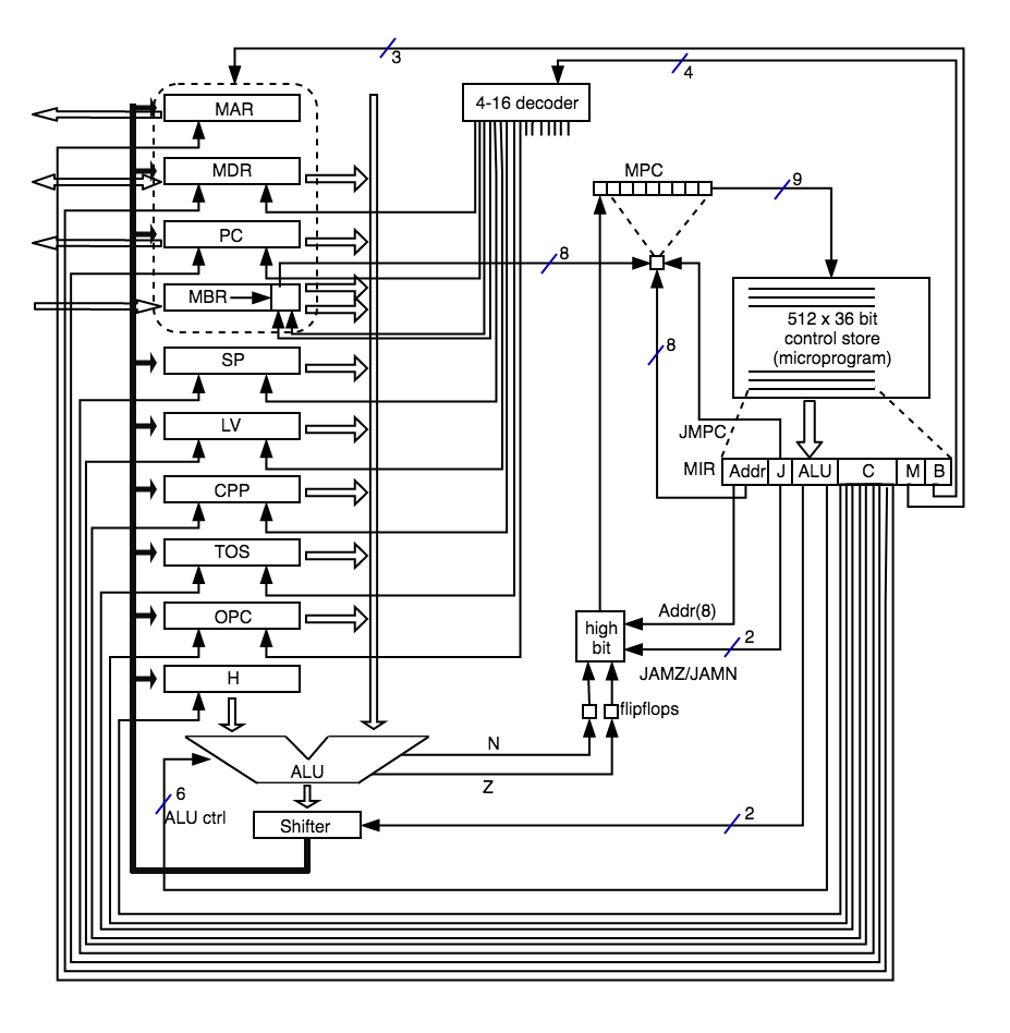
In Andrew Tananbaum’s wonderful book ‘Structured Computer Organization’ a microarchitecture called Mic-1 is presented, which can be easily understood with all aspects we have seen so far. It is designed for educational purposes, but allows us to zoom in on many relevant aspects.

Briefly:
- Mic-1 has ten 32-bit registers.
- PC is the ISA program counter
- MAR, MDR and MBR are used to communicate with memory (see below)
- SP and LV are the stack pointer and pointer local variables (stack frame)
- CPP contains a pointer in memory to all constants in a program
- TOS is the top-of-stack, kept in a register to gain speed
- OPC is the ISA instruction register
- H contains intermediate results
- Program Counter (MPC) points into memory. Every cycle 36 bits are copied to MIR (fetch) to drive the µArch (decode)
- Different fields in MIR drive different parts of the µarch
- Two registers are loaded into the ALU. To keep Mic-1 simple, one is always H (half-result). For instance, 5*6+7 would be computed first by loading 5 in H, then multiplying H with 6 (from memory), writing the result 30 in H, and then adding 7 to H.
- So precisely one register must be loaded through the B bus into the ALU every cycle. Therefore the B field has an index which is decoded to one of 9 registers.
- The result of a computation can be loaded in more than one register, so the C field isn’t decoded, but controls 9 registers independently to accept the value from the C-bus
- The ALU accepts 6 control lines and 2 lines to an (independent) shifter. 6 bits allows for 64 operations in total, which include and, or, xor, not, +, -, *, /, increment, decrement, etcetera
- The shifter allows an additional shift within the same cycle, which allows (among other things) to cycle conveniently through all bits of a value
- The N and Z outputs reflect if the result of a numeric computation is negative or zero, respectively. These results are stored in flip-flops (memory) to be used in the next instruction. In this way conditional jumps (if, for, while) simply use this status
- Unlike ISA instructions, every µinstruction contains the address of the next instruction and JAMZ and JAMN bits to determine if the N and Z flags will be used (i.e., a conditional jump). If so, the high bit of the next address is (re)set. This means both the true-part and the false-part are reached without additional jump!
Mic-1 communicates with memory in two ways: 8-bit data or 32-bit words. The first is used to fetch ISA instructions: the ISA PC is used as address to fetch one byte into the low part of MBR. While that is fetched, the PC is incremented in one cycle. MAR is a word address, meaning that four bytes of ISA data are fetched or stored at once to/from MDR. Two control lines signal memory read/write through MAR/MDR; one control line signals memory read through PC/MBR
Conclusion
Starting from the humble beginnings of the transistor we have now been able to sketch the working of a µArchitecture, and through that hinted at the workings of modern processors.
Several aspects haven’t yet been looked at. We will discuss
- Language Processing
We have used the word ‘interpretation’ loosely, but we will briefly go into language processing in general; - Parallelism
In order to achieve ever greater performance, CPU’s continue to be engineered. The most important manner to do so is to device ways in which more computation can occur at the same time, by parallelization; - Virtual Memory
Regarding memory as an array of bytes is an oversimplification; - Multi-tasking
Finally, how can processors execute thousands of programs seeming at the same time, and how do they make use of the huge storage at their disposal
